Structure of n-type gallium oxide Schottky diode with adjustable potential barrier and preparation method thereof
阅读说明:本技术 势垒可调的n型氧化镓肖特基二极管的结构及其制备方法 (Structure of n-type gallium oxide Schottky diode with adjustable potential barrier and preparation method thereof ) 是由 汪海波 杨金 樊敏 张忠祥 鲁世斌 陆梦雪 汪承龙 于 2021-07-20 设计创作,主要内容包括:本发明属于半导体技术领域,且公开了势垒可调的n型氧化镓肖特基二极管的结构及其制备方法,二极管由上到下依次包括阳极金属层、阳极场板、介质层、势垒调控层、低掺杂氧化镓外延层和衬底层以及阴极金属层,所述的势垒调控层厚度小于20nm,浓度在2e16~2e20atom/cm3。本发明,通过设置不改变反向击穿性能的同时,增加二极管多子的发射能力,从而提高功率密度,降低导通电阻。(The invention belongs to the technical field of semiconductors and discloses a barrier-adjustable n-type gallium oxide Schottky diode structure and a preparation method thereof, wherein the diode sequentially comprises an anode metal layer, an anode field plate, a dielectric layer, a barrier regulation layer, a low-doped gallium oxide epitaxial layer, a substrate layer and a cathode metal layer from top to bottom, the thickness of the barrier regulation layer is less than 20nm, and the concentration is 2e 16-2 e20atom/cm 3. According to the invention, the emission capability of the diode is increased while the reverse breakdown performance is not changed, so that the power density is improved, and the on-resistance is reduced.)
1. The structure of the potential barrier adjustable n-type gallium oxide Schottky diode comprises an anode metal layer (31), an anode field plate (37), a dielectric layer (32), a potential barrier regulation layer (33), a low-doped gallium oxide epitaxial layer (34), a substrate layer (35) and a cathode metal layer (36), and is characterized in that: the top of the anode field plate (37) is matched with the top of the anode metal layer (31) for use, the outer surface of the anode metal layer (31) is matched with the inside of the dielectric layer (32) for use, the bottom of the dielectric layer (32) is matched with the top of the barrier regulating layer (33) for use, the bottom of the barrier regulating layer (33) is matched with the top of the low-doped gallium oxide epitaxial layer (34) for use, the bottom of the low-doped gallium oxide epitaxial layer (34) is matched with the top of the substrate layer (35) for use, and the bottom of the substrate layer (35) is matched with the top of the cathode metal layer (36) for use.
2. The structure of the barrier tunable n-type gallium oxide schottky diode of claim 1 wherein: the anode metal layer (31) and the anode field plate (37) are made of the same metal, and the anode metal layer (31) is made of one of Cu, Ag, Pt, Ni and Au.
3. The barrier tunable n-type gallium oxide schottky diode structure and the method of making the same as claimed in claim 1, wherein: the barrier regulation layer (33) is an n-type high-concentration gallium oxide thin layer, doping impurities of the n-type high-concentration gallium oxide thin layer are Sn or Si, the concentration is 2e 16-2 e20atom/cm3, the optimal range is 5e 17-5 e19atom/cm3, the doping thickness of the n-type high-concentration gallium oxide thin layer is 1-20 nm, and the optimal range is 1-10 nm.
4. The method of making a barrier tunable n-type gallium oxide schottky diode according to claim 1, comprising the steps of:
the first step is as follows: selecting a high-concentration n-type doped gallium oxide substrate;
the second step is that: extending a low-doping-concentration n-type gallium oxide layer on a high-concentration gallium oxide substrate;
the third step: extending a high-doping-concentration n-type gallium oxide barrier regulation thin layer on the low-concentration gallium oxide epitaxial layer;
the fourth step: evaporating a cathode metal layer on the back of the high-concentration gallium oxide substrate;
the fifth step: depositing a dielectric layer on the gallium oxide barrier regulation layer;
and a sixth step: coating glue on the dielectric layer, exposing, photoetching and etching once to form an anode metal opening pattern;
the seventh step: evaporating anode metal in the opening pattern to form Schottky contact of the metal barrier regulation layer;
eighth step: and on the basis of evaporating the metal, exposing and photoetching again to evaporate the metal field plate.
5. The method of making a barrier tunable n-type gallium oxide schottky diode of claim 4 wherein: the thickness of the anode metal is 20-2000 nm, and the thickness of the field plate is 20-2000 nm.
6. The method of making a barrier tunable n-type gallium oxide schottky diode of claim 4 wherein: the area of the field plate is 40% larger than that of the anode, and the distance between the edge of the field plate and the edge of the anode is more than 200 nm.
7. The method of making a barrier tunable n-type gallium oxide schottky diode of claim 4 wherein: the dielectric layer (32) is made of silicon oxide, silicon nitride, aluminum oxide and alumina, and preferably is made of aluminum oxide.
8. The method of making a barrier tunable n-type gallium oxide schottky diode of claim 4 wherein: the thickness of the dielectric layer is 20 nm-2000 nm.
Technical Field
The invention belongs to the technical field of semiconductors, and particularly relates to a structure of a potential barrier adjustable n-type gallium oxide Schottky diode and a preparation method thereof.
Background
Silicon-based devices have not been able to meet the increasing technical demands of high energy density and high frequency in the context of high speed rail and 5G applications, and silicon carbide and gallium nitride, which are typical materials of third generation semiconductors, are becoming more and more the focus of current society and research institutes because they have large forbidden band widths and high breakdown electric fields, thereby hopefully overcoming the technical limitations of silicon devices, however, due to the limitations of crystal growth, difficulty and cost of device fabrication, these materials have not been widely used to date.
Gallium oxide is a new semiconductor candidate material, and has a wider forbidden band and a higher breakdown voltage; schottky Barrier Diodes (SBDs) with low on-voltage, high forward current density and high switching speed characteristics can be developed on a homogeneous or heterogeneous substrate; the Chinese invention patent CN111192927A discloses a gallium oxide Schottky diode and a manufacturing method thereof, which has a low-doped epitaxial layer and a gallium oxide substrate and can improve the influence of an interface state on the leakage current of a device; the Chinese invention patent CN106876484B discloses a Schottky diode with high breakdown voltage and a manufacturing method thereof, wherein a 300-500 nm organic iron dielectric layer is deposited on an epitaxial layer of the Schottky diode, so that the reverse breakdown voltage can be improved; the Chinese invention patent CN107026209A also discloses a junction barrier Schottky diode based on gallium oxide and a preparation method thereof, wherein a p-n junction barrier is adopted to form a larger power semiconductor device, but the p-type gallium oxide is difficult to manufacture; chinese invention patents CN201822033721.9 and CN202011125271.1 also disclose the structure and the preparation method of the gan schottky diode.
The anode of the Schottky diode can be made of various materials, including metals with higher work functions such as Cu, Ag, Pt, Ni and Au, and the prepared diodes have different performances, and the preparation process and the flow are difficult to unify, so that the types and the cost are different.
Disclosure of Invention
Aiming at the problems in the prior art, the invention provides a barrier-adjustable n-type gallium oxide Schottky diode structure which comprises an anode metal layer, an anode field plate, a dielectric layer, a barrier regulation layer, a low-doped gallium oxide epitaxial layer, a substrate layer and a cathode metal layer, wherein the top of the anode field plate is matched with the top of the anode metal layer, the outer surface of the anode metal layer is matched with the inside of the dielectric layer, the bottom of the dielectric layer is matched with the top of the barrier regulation layer, the bottom of the barrier regulation layer is matched with the top of the low-doped gallium oxide epitaxial layer, the bottom of the low-doped gallium oxide epitaxial layer is matched with the top of the substrate layer, and the bottom of the substrate layer is matched with the top of the cathode metal layer.
Preferably, the anode metal layer and the anode field plate are made of the same metal, and the anode metal layer is made of one of Cu, Ag, Pt, Ni and Au.
Preferably, the barrier control layer is an n-type high-concentration gallium oxide thin layer, the doping impurity of the n-type high-concentration gallium oxide thin layer is Sn or Si, and the concentration of the doping impurity is 2e 16-2 e20atom/cm3The most preferable range is 5e 17-5 e19atom/cm3And the doping thickness of the n-type high-concentration gallium oxide thin layer is 1-20 nm, and the optimal range is 1-10 nm.
As is preferred in the context of the present invention,
the first step is as follows: selecting a high-concentration n-type doped gallium oxide substrate;
the second step is that: extending a low-doping-concentration n-type gallium oxide layer on a high-concentration gallium oxide substrate;
the third step: extending a high-doping-concentration n-type gallium oxide barrier regulation thin layer on the low-concentration gallium oxide epitaxial layer;
the fourth step: evaporating a cathode metal layer on the back of the high-concentration gallium oxide substrate;
the fifth step: depositing a dielectric layer on the gallium oxide barrier regulation layer;
and a sixth step: coating glue on the dielectric layer, exposing, photoetching and etching once to form an anode metal opening pattern;
the seventh step: evaporating anode metal in the opening pattern to form Schottky contact of the metal barrier regulation layer;
eighth step: and on the basis of evaporating the metal, exposing and photoetching again to evaporate the metal field plate.
Preferably, the thickness of the anode metal is 20-2000 nm, and the thickness of the field plate is 20-2000 nm.
Preferably, the area of the field plate is 40% larger than that of the anode, and the distance between the edge of the field plate and the edge of the anode is more than 200 nm.
Preferably, the dielectric layer is silicon oxide, silicon nitride, aluminum oxide, or hafnium oxide, and preferably is aluminum oxide.
Preferably, the dielectric layer has a thickness of 20nm to 2000 nm.
Compared with the prior art, the invention has the following beneficial effects:
1. according to the invention, the n-type gallium oxide barrier thin layer with high concentration is adopted, the thickness of the thin layer is less than 20nm, the n-type barrier thin layer of the thin layer can promote tunnel current, reduce Schottky effective contact barrier, obviously reduce on-resistance, increase power density and reduce power consumption;
2. the Schottky diodes with various power purposes can be realized under the condition of the same metal anode, and the process flow is simplified. The Schottky diode disclosed by the invention is provided with the n-type high-concentration doped gallium oxide barrier regulation and control layer, the current density can be obviously changed by the regulation and control layer, the barrier height is reduced, and the on-resistance is reduced, so that the high-power density adjustable Schottky diode is realized.
Drawings
Fig. 1 is a schematic diagram of the relationship between the thickness of Ni and the barrier obtained by using Ni as the anode, according to the effective barrier control effect of the gan barrier control layer on the schottky diode provided in the embodiment of the present invention;
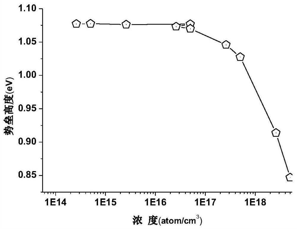
fig. 2 shows the effective barrier control effect of the gan barrier control layer on the schottky diode according to the embodiment of the present invention, and the relationship between the Ni concentration and the barrier obtained by using Ni as the anode;
fig. 3 is a schematic cross-sectional view of a gan schottky diode according to an embodiment of the present invention;
fig. 4 is a flowchart of a method for manufacturing a gan schottky diode according to an embodiment of the present invention.
Detailed Description
In order to further understand the contents, features and effects of the present invention, the following embodiments are illustrated and described in detail with reference to the accompanying drawings.
The structure of the present invention will be described in detail below with reference to the accompanying drawings.
Fig. 3 shows a schematic cross-sectional view of a gan schottky diode, which is shown from top to bottom with an anode field plate 37 and an anode metal layer 31, a dielectric layer 32, a high concentration n-type gan barrier control layer 33, a low doped n-type gan epitaxial layer 34, a high concentration substrate layer 35 and a cathode metal layer 36.
The anode field plate 37 and the anode metal layer 31 are made of the same material, and can be made of metal with a work function higher than gallium oxide, such as Ni, Pt, Cu, Ag, Au, and the like, if Ni is used, Au needs to be added to prevent oxidation, and the anode metal is located on the upper portion of the dielectric layer 32, penetrates through the dielectric layer 32 to form schottky contact, and the anode field plate 37 has a longitudinal section size of 20000nm, a thickness of 1500nm, a longitudinal section size of 2000nm and a thickness of 500 nm.
The dielectric layer 32 may be one of silicon oxide, silicon nitride, hafnium oxide and aluminum oxide, and has a thickness of 500 nm;
wherein the high-concentration n-type gallium oxide barrier regulation layer 33 is doped with Sn or Si, has a thickness of 10nm and a concentration of 2.6e18atom/cm3;
Wherein, the low-doped n-type gallium oxide epitaxial layer 34 is also realized by doping Si or Sn with the concentration of 2e16atom/cm3The thickness is 2 um;
wherein, the high concentration n-type gallium oxide substrate 35 is also realized by doping Si or Sn, and the concentration is 3.6e18atom/cm3The thickness is 200 um;
by adopting Ni as anode metal and testing, the conduction voltage of the embodiment is 0.75V, the effective barrier height is 0.84eV, and the forward current density can reach 10V at 0.8V2A/cm2The test result will vary according to the test conditions, but compared with the same condition without the barrier adjusting layer 33,the current density is greatly improved.
The embodiment of the invention provides a manufacturing method of a gallium oxide Schottky diode.
Step 41, selecting a high-concentration doped n-type gallium oxide substrate; in the present case, the concentration range e18atom/cm is used3The surface is polished to a mirror surface by a chemical mechanical polishing method.
Step 42 is to extend the low doping concentration n-type gallium oxide layer; the doping concentration range is e 14-e 18atom/cm3Range, the longitudinal concentration distribution is uniform doping; the epitaxial method may be chemical vapor deposition.
Step 43 is to epitaxially dope a high concentration n-type oxidizer layer; the doping concentration is e 17-e 19atom/cm3The doping equipment can use hydride vapor phase epitaxy or metal oxide chemical vapor deposition, and the deposition thickness is 1-20 nm.
And 44, evaporating the back cathode metal to form ohmic contact, wherein the cathode metal is prepared by adopting a Ti layer and covering Au as a protective layer through an electron beam evaporation method.
And step 45, depositing a dielectric layer on the high-concentration barrier layer, wherein the dielectric layer is one of silicon oxide, silicon nitride, hafnium oxide and aluminum oxide, the adopted preparation method can be plasma enhanced chemical vapor deposition and low-pressure chemical vapor deposition, and the deposition thickness is 20-2000 nm.
Step 46 is to form an anode window by one-time photoetching, and specifically comprises gluing, exposing and etching on the dielectric layer. The photoresist is corrosion-resistant photoresist, an opening area is formed on the dielectric layer through exposure, an opening pattern is circular, the diameter of the circular opening is 2 microns, and then the dielectric layer of the exposed area is removed through a dry-wet combination method.
Step 47 is to evaporate the anode metal, and in the open pore region, the anode schottky contact is formed by electron beam evaporation, and the evaporation thickness is calculated by the evaporation rate, and the metal can be one of Ni, Pt, Ag, Cu, and Pt, and at this time, it is not necessary to evaporate Au as a protection layer.
And step 48, forming a field plate window by secondary photoetching, coating glue and exposing again on the basis of removing the previous photoresist, wherein the exposed area of the secondary photoetching corresponds to the anode of the primary exposure, the area is far larger than the area of the anode, the pattern is circular, and the diameter is 20 microns.
Step 49 re-evaporates the metal, which is the same as the metal of step 47, to a thickness of 1500 nm. If the metal is selected to be easy to oxidize, the product Au can be continuously used as a protective layer. And finally removing the photoresist.
It is noted that, herein, relational terms such as first and second, and the like may be used solely to distinguish one entity or action from another entity or action without necessarily requiring or implying any actual such relationship or order between such entities or actions. Also, the terms "comprises," "comprising," or any other variation thereof, are intended to cover a non-exclusive inclusion, such that a process, method, article, or apparatus that comprises a list of elements does not include only those elements but may include other elements not expressly listed or inherent to such process, method, article, or apparatus.
Although embodiments of the present invention have been shown and described, it will be appreciated by those skilled in the art that changes, modifications, substitutions and alterations can be made in these embodiments without departing from the principles and spirit of the invention, the scope of which is defined in the appended claims and their equivalents.
- 上一篇:一种医用注射器针头装配设备
- 下一篇:一种碳化硅TMBS器件结构及其制造方法