Silicon carbide TMBS device structure and manufacturing method thereof
阅读说明:本技术 一种碳化硅tmbs器件结构及其制造方法 (Silicon carbide TMBS device structure and manufacturing method thereof ) 是由 温正欣 喻双柏 郑泽东 和巍巍 于 2021-08-31 设计创作,主要内容包括:本发明公开了一种碳化硅TMBS器件结构。所述结构包括一n型掺杂碳化硅衬底,其上方有一n型掺杂碳化硅外延层,在碳化硅外延层的顶部有若干沟槽,所述沟槽的侧壁和底部有氧化层,所述沟槽中填充有p型掺杂多晶硅,每两个相邻的沟槽之间有p型沟槽保护区,p型沟槽保护区包裹对应的两个沟槽的内边缘。本发明同时公开了该器件的制造方法。与常规的TMBS器件结构及制造方法相比,本发明结合了碳化硅材料的特点,通过引入沟槽保护区的结构,以在正向大电流状态下起到双极型导通的作用,提高了器件允许的最大浪涌电流。(The invention discloses a silicon carbide TMBS device structure. The structure comprises an n-type doped silicon carbide substrate, an n-type doped silicon carbide epitaxial layer is arranged above the n-type doped silicon carbide substrate, a plurality of grooves are formed in the top of the silicon carbide epitaxial layer, oxide layers are arranged on the side wall and the bottom of each groove, p-type doped polycrystalline silicon is filled in each groove, a p-type groove protection area is arranged between every two adjacent grooves, and the p-type groove protection areas wrap the inner edges of the two corresponding grooves. The invention also discloses a manufacturing method of the device. Compared with the conventional TMBS device structure and the manufacturing method, the invention combines the characteristics of the silicon carbide material, and plays a role of bipolar conduction in a forward large current state by introducing the structure of the groove protection area, thereby improving the maximum surge current allowed by the device.)
1. The utility model provides a carborundum TMBS device structure, its characterized in that includes an n type doping carborundum substrate, and there is an n type doping carborundum epitaxial layer above it, has a plurality of slots at the top of carborundum epitaxial layer, the lateral wall and the bottom of slot have the oxide layer, it has p type doping polycrystalline silicon to fill in the slot, has p type slot guard zone between every two adjacent slots, and p type slot guard zone parcel corresponds the inward flange of two slots.
2. The silicon carbide TMBS device structure of claim 1, wherein the p-type trench protection regions have a depth greater than the depth of the trenches and wrap around the inner edges of the corresponding two trenches on the side where they are close to each other.
3. The silicon carbide TMBS device structure of claim 1, wherein the trench has a depth of 0.5 μ ι η to 1 μ ι η.
4. The silicon carbide TMBS device structure of claim 1, wherein the oxide layer has a thickness of 30nm to 100 nm.
5. A method of fabricating a silicon carbide TMBS device, comprising the steps of:
s1, growing a silicon carbide epitaxial layer on the silicon carbide substrate;
s2, performing P-type ion implantation to form a plurality of P-type implantation regions on the top of the silicon carbide epitaxial layer;
s3, etching grooves on two sides of each P-type injection region through an etching process, and partially etching the grooves in the P-type injection regions;
s4, forming an oxide layer on the side wall and the bottom of the groove through an oxidation process;
s5, depositing p-type doped polycrystalline silicon on the surface of the structure to fill the groove;
and S6, sputtering Schottky contact metal on the front surface of the structure, sputtering ohmic contact metal on the back surface of the structure, and forming a silicon carbide TMBS device structure after laser annealing.
6. The method of claim 5, wherein in step S2, Al ion implantation is used, the maximum energy of implantation is 800keV or more, and the depth of the p-type implantation region is 1.2 μm to 2 μm.
7. The method of manufacturing a silicon carbide TMBS device of claim 5, wherein the depth of the trench is less than the depth of the p-type implanted region.
Technical Field
The invention belongs to the technical field of semiconductor devices, and particularly relates to a silicon carbide TMBS device structure and a manufacturing method thereof.
Background
The silicon carbide schottky diode is a silicon carbide-based power electronic device structure which is commercialized at the earliest time, and is widely used in the fields of communication power supplies, photovoltaic inversion and the like due to excellent device performance. The traditional silicon carbide Schottky diode is of a planar structure, and an electric field at the top of the device is reduced by utilizing a p-type region injected at the top of a drift region; under the surge working condition, the np junction of the p-type injection region and the n-type drift region is opened, and large surge current is conducted.
The groove type JBS device is an improved silicon carbide Schottky diode structure, and a surface electric field in a blocking state is further reduced by using a groove + p-type injection method, so that a drift region of the device can adopt higher doping concentration, and the conduction characteristic of the device is improved. However, the trench-type JBS device structure only reduces the maximum field strength at the contact surface and does not increase the breakdown voltage of the silicon carbide drift region.
In a silicon device, the latest schottky diode device structure is a trench type MOS barrier schottky diode (TMBS), which uses the charge coupling effect of a MOS barrier formed between a trench electrode and an epitaxial layer, and can use the epitaxial layer with higher doping concentration on the basis that the device bears unchanged reverse withstand voltage, thereby greatly reducing the on-state resistance of the device and breaking through the unipolar performance limit of the material.
However, the TMBS structure of a silicon device cannot be transferred directly to a silicon carbide device, mainly for two reasons: firstly, a silicon carbide device is used for preparing TMBS with a traditional structure, and silicon dioxide can be broken down in advance in a blocking state; second, the conventional TMBS structure has no bipolar current path, has poor surge characteristics, and is not significant in silicon devices, but is a prominent defect in silicon carbide devices.
Disclosure of Invention
The invention provides a silicon carbide TMBS device structure and a manufacturing method thereof, which utilize a charge coupling effect to reduce the surface electric field of Schottky contact, improve the doping concentration of an epitaxial layer and reduce the on-state resistance of the device, and reduce the maximum field intensity of gate oxide in a blocking state by introducing a groove protection structure, wherein the protection structure simultaneously plays a role of a surge current bipolar channel, and improves the surge capacity of the device.
In a first aspect, the invention provides a 3C silicon carbide device structure on a silicon substrate, including an n-type doped silicon carbide substrate, an n-type doped silicon carbide epitaxial layer is provided above the n-type doped silicon carbide substrate, a plurality of trenches are provided on the top of the silicon carbide epitaxial layer, oxide layers are provided on the sidewalls and the bottom of the trenches, p-type doped polysilicon is filled in the trenches, a p-type trench protection region is provided between every two adjacent trenches, and the p-type trench protection region wraps the inner edges of the two corresponding trenches.
Preferably, the depth of the p-type groove protection region is greater than that of the groove, and the p-type groove protection region wraps the inner edge of one side of the two corresponding grooves close to each other.
Preferably, the depth of the trench is 0.5 μm to 1 μm.
Preferably, the thickness of the oxide layer is 30nm to 100 nm.
In another aspect of the present invention, the present invention provides a method for manufacturing a silicon carbide TMBS device, comprising the steps of:
s1, growing a silicon carbide epitaxial layer on the silicon carbide substrate;
s2, performing P-type ion implantation to form a plurality of P-type implantation regions on the top of the silicon carbide epitaxial layer;
s3, etching grooves on two sides of each P-type injection region through an etching process, and partially etching the grooves in the P-type injection regions;
s4, forming an oxide layer on the side wall and the bottom of the groove through an oxidation process;
s5, depositing p-type doped polycrystalline silicon on the surface of the structure to fill the groove;
and S6, sputtering Schottky contact metal on the front surface of the structure, sputtering ohmic contact metal on the back surface of the structure, and forming a silicon carbide TMBS device structure after laser annealing.
Preferably, in step S2, Al ion implantation is used, the implantation maximum energy is above 800keV, making the depth of the p-type implantation region 1.2 μm to 2 μm.
Preferably, the depth of the trench is less than the depth of the p-type implantation region.
Compared with the prior art, the silicon carbide TMBS device has the beneficial effects that:
compared with the common silicon carbide JBS device, the charge coupling structure is introduced, the surface electric field of the device is reduced, the epitaxial layer can select higher doping concentration, and the on-state resistance of the device is reduced. Compared with the conventional TMBS device structure, the trench protection structure has the advantages that the trench protection structure is introduced to play a role in bipolar conduction in a forward high-current state by combining the characteristics of the silicon carbide material, and the maximum surge current allowed by the device is increased.
Drawings
In order to more clearly illustrate the technical solutions in the embodiments of the present invention, the drawings used in the description of the embodiments will be briefly introduced below, and it is obvious that the drawings shown below are only some embodiments of the present invention and are not intended to limit the present invention.
FIG. 1 is a schematic diagram of a silicon carbide TMBS device structure according to one embodiment of the invention;
FIG. 2 is a flow chart of a method of fabricating a silicon carbide TMBS device in accordance with one embodiment of the invention;
fig. 3-7 are schematic diagrams of device structures resulting from different steps of a silicon carbide TMBS device fabrication method according to an embodiment of the present invention.
Description of the main elements
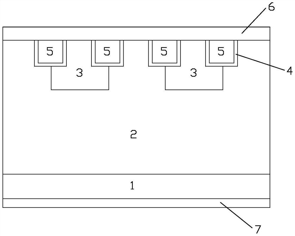
Silicon carbide substrate 1
Silicon carbide epitaxial layer 2
Trench protection region 3
P-type implant region 31
Oxide layer 4
Groove 41
p-type doped polysilicon 5
Schottky contact metal 6
Ohmic contact metal 7
The following detailed description will further illustrate the invention in conjunction with the above-described figures.
Detailed Description
In order to make the objects, technical solutions and advantages of the present invention more apparent, the present invention will be described in further detail with reference to the accompanying drawings and specific embodiments. It should be understood that the specific embodiments described herein are merely illustrative of the invention and are not intended to limit the invention.
Referring to fig. 1, in one aspect, embodiments of the present invention provide a silicon carbide TMBS device structure. In the embodiment, the silicon carbide TMBS device structure comprises an n-type doped silicon carbide substrate (1), an n-type doped silicon carbide epitaxial layer (2) is arranged above the n-type doped silicon carbide substrate, a plurality of grooves are arranged at the top of the silicon carbide epitaxial layer (2), the depth of each groove is 0.5-1 μm, the width of each groove is 0.5-2 μm, and the distance between every two adjacent grooves is 2-4 μm; an oxide layer (4) is arranged on the side wall and the bottom of the groove, and the thickness of the oxide layer (4) is 30nm to 100 nm; p-type doped polycrystalline silicon (5) is filled in the groove; a p-type groove protection region (3) is arranged between every two adjacent grooves, and the p-type groove protection regions (3) wrap the inner edges of the two corresponding grooves.
In the embodiment, the depth of the p-type groove protection region (3) is 1.2-2 μm, the depth of the p-type groove protection region (3) is larger than that of the groove, and the p-type groove protection region (3) wraps the inner edge of one side of the two corresponding grooves, which are close to each other.
Compared with a conventional TMBS device structure, the silicon carbide TMBS device structure provided by the invention is additionally provided with the groove protection region (3), so that the effect of protecting a groove oxidation layer is achieved in a blocking state, and the effect of opening a PN junction and providing a bipolar current path is achieved in a high-current conduction state.
Referring to fig. 2, an embodiment of the present invention provides a method for manufacturing a silicon carbide TMBS device, including the steps of:
step S1: an epitaxial layer (2) of silicon carbide is grown on a silicon carbide substrate (1) to form the structure shown in fig. 3.
Step S2: carrying out P-type ion implantation on the surface of the silicon carbide epitaxial layer (2) to form a plurality of P-type implantation regions (31) on the top of the silicon carbide epitaxial layer (2); in this embodiment, the ion implantation is performed by using Al ion implantation, and the maximum implantation energy is 800keV or more, so that the depth of the p-type implantation region (31) is 1.2 to 2 μm, thereby forming the structure shown in fig. 4.
Step S3: etching the top of the silicon carbide epitaxial layer (2) to form a groove (41) on each of two sides of each P-type injection region (31), wherein the groove (41) is partially etched in the P-type injection region (31) to form a P-type groove protection region (3) in the remaining P-type injection region; the depth of the trench (41) is less than the depth of the p-type implantation region (31); preferably, the depth of the trench (41) may be 0.5 μm to 1 μm; the trench etch gas may be selected from SF6, O2, and HBr in a gas ratio of 5:1:6 to form the structure shown in fig. 5.
Step S4: oxidizing the silicon carbide structure to form an oxide layer (4) on the sidewall and bottom of the trench (41); wherein the oxidation temperature is 1250 ℃ to 1350 ℃, and the thickness of the oxidation layer is 30nm to 100nm, thereby forming the structure shown in figure 6.
Step S5: and depositing p-type doped polysilicon (5) on the surface of the structure to fill the trench (41) to form the structure shown in FIG. 7.
Step S6: and sputtering Schottky contact metal (6) on the front surface of the device structure, sputtering ohmic contact metal (7) on the back surface of the device structure, and performing laser annealing to form the silicon carbide TMBS device structure shown in figure 1.
The foregoing is a more detailed description of the invention in connection with specific/preferred embodiments and is not intended to limit the practice of the invention to those descriptions. It will be apparent to those skilled in the art that various substitutions and modifications can be made to the described embodiments without departing from the spirit of the invention, and these substitutions and modifications should be considered to fall within the scope of the invention. In the description herein, references to the description of the term "one embodiment," "some embodiments," "preferred embodiments," "an example," "a specific example," or "some examples" or the like are intended to mean that a particular feature, structure, material, or characteristic described in connection with the embodiment or example is included in at least one embodiment or example of the invention. In this specification, the schematic representations of the terms used above are not necessarily intended to refer to the same embodiment or example. Furthermore, the particular features, structures, materials, or characteristics described may be combined in any suitable manner in any one or more embodiments or examples. Furthermore, various embodiments or examples and features of different embodiments or examples described in this specification can be combined and combined by one skilled in the art without contradiction.
- 上一篇:一种医用注射器针头装配设备
- 下一篇:一种封装盖板及其制作方法、光伏组件