Porous GaN narrow-band ultraviolet photodiode and preparation method thereof
阅读说明:本技术 一种多孔GaN窄带紫外光电二极管及其制备方法 (Porous GaN narrow-band ultraviolet photodiode and preparation method thereof ) 是由 宋伟东 郭越 吴明建 梁众 林显凯 陈钊 高岩 张业龙 何鑫 于 2021-07-20 设计创作,主要内容包括:本发明提供一种多孔GaN窄带紫外光电二极管及其制备方法,包括衬底层;设置于衬底层上的半导体层,设置于半导体层上表面的多孔GaN层和CuZnS层;分别设置于多孔GaN层和CuZnS层上表面的金属触点层。本发明通过在衬底层上沉积GaN薄膜;对GaN薄膜进行清洗,并用离子液刻蚀GaN薄膜一部分,形成多孔GaN层;将GaN薄膜另一部分用水浴法在表面制得CuZnS层。本发明利用多孔GaN材料作为紫外光吸收层,改善光吸收降低材料缺陷;本发明利用的P型透明、高导电薄膜CuZnS具备了ZnS的高透过率和CuS的高导电特性;多孔GaN窄带紫外光电二极管半峰宽仅5nm,紫外响应波段为362~380nm,并具有高探测率,适用于弱光窄带光谱检测。(The invention provides a porous GaN narrow-band ultraviolet photodiode and a preparation method thereof, wherein the porous GaN narrow-band ultraviolet photodiode comprises a substrate layer; the semiconductor layer is arranged on the substrate layer, and the porous GaN layer and the CuZnS layer are arranged on the upper surface of the semiconductor layer; and the metal contact layers are respectively arranged on the upper surfaces of the porous GaN layer and the CuZnS layer. The invention deposits GaN film on the substrate layer; cleaning the GaN film, and etching a part of the GaN film by using ionic liquid to form a porous GaN layer; and preparing a CuZnS layer on the surface of the other part of the GaN film by a water bath method. The invention uses the porous GaN material as the ultraviolet light absorption layer, improves the light absorption and reduces the material defects; the P-type transparent and high-conductivity film CuZnS has the high transmittance of ZnS and the high conductivity of CuS; the half-peak width of the porous GaN narrow-band ultraviolet photodiode is only 5nm, the ultraviolet response waveband is 362-380 nm, and the porous GaN narrow-band ultraviolet photodiode has high detectivity and is suitable for weak light narrow-band spectrum detection.)
1. The porous GaN narrow-band ultraviolet photodiode is characterized by comprising a substrate layer (100), a semiconductor layer (200), a porous GaN layer (300), a CuZnS layer (400) and a metal contact layer (500), wherein the semiconductor layer (200) is arranged on the upper surface of the substrate layer (100), and the semiconductor layer (200) is a GaN thin film layer;
the semiconductor layer (200) is provided with a porous GaN layer (300) and a CuZnS layer (400), and the upper surfaces of the porous GaN layer (300) and the CuZnS layer (400) are provided with metal contact layers (500).
2. The porous GaN narrow band uv photodiode of claim 1, wherein: the substrate layer 100 is a sapphire substrate layer.
3. The porous GaN narrow band uv photodiode of claim 1, wherein: the GaN thin film layer has a carrier concentration range of 1 × 10 at room temperature15To 1X 1018cm-3The thickness is 4-6 μm.
4. The porous GaN narrow band uv photodiode of claim 1, wherein: the thickness of the CuZnS layer 400 is 30-100 nm.
5. The porous GaN narrow band uv photodiode of claim 1, wherein: the metal contact layer 500 is an ohmic contact layer, and the thickness of the ohmic contact layer is 50-200 nm.
6. A method for fabricating the porous GaN narrow band ultraviolet photodiode of any of claims 1-5, the method comprising:
s1), depositing a GaN film on the substrate layer (100);
s2), cleaning the GaN film prepared in the step S1), and etching a part of the GaN film by using ionic liquid to form a porous GaN layer (300);
s3), another part of the GaN thin film was formed into a CuZnS layer (400) on the surface by a water bath method.
7. The method for preparing a porous GaN narrow band UV photodiode of claim 6, wherein in step S2), before etching the porous GaN layer (300), the thickness of the porous GaN layer is 0.2-0.5cm2Placing the GaN in aqua regia to remove the passivation layer on the surface;
then, ultrasonically cleaning the GaN sheet in acetone, ethanol and deionized water in sequence;
and then carrying out hydrophilic treatment on the GaN sheet in an ultraviolet ozone cleaning machine to enhance the contact between the GaN sheet and the etchant, wherein the hydrophilic treatment time is 10-30 min.
8. The method for preparing a porous GaN narrow-band ultraviolet photodiode as recited in claim 6, wherein the ionic liquid used in step S2) is: 1-ethyl-3-methylimidazole trifluoromethanesulfonate or 1-ethyl-3-methylimidazole trifluoroacetate.
9. The method for preparing a porous GaN narrow-band ultraviolet photodiode according to claim 6, wherein the specific preparation method of the porous GaN layer (300) in step S2) is as follows:
s201), using the InGa alloy as an electrode, and enabling the electrode and the GaN sheet to form ohmic contact;
s202), connecting a GaN sheet with the positive electrode of a power supply, connecting a platinum sheet with the negative electrode, placing and fixing the two electrodes in parallel on an iron support, placing the electrodes in the position of about 10-30cm in front of a xenon lamp, and enabling the etched surface of the GaN to face the xenon lamp;
s203), soaking the GaN sheet and the platinum sheet in a beaker filled with ionic liquid, setting the voltage of a direct current power supply to be 10-25V, and etching for 5-20 min.
10. The method for manufacturing a porous GaN narrow band uv photodiode according to claim 6, wherein the specific method for manufacturing the CuZnS layer (400) in step S3) is:
s301) preparing three precursor solutions
Solution A: 0.03g to 0.12g of copper sulfate and 1g to 2g of zinc acetate are mixed in 100 and 200ml of deionized water;
solution B: mixing 0.5-1g disodium ethylene diamine tetraacetate with 100ml deionized water;
solution C: 0.5-1g of C2H5Mixing NS and 50-200ml deionized water for dissolving;
s302), then mixing the solution B with the solution A and carrying out ultrasonic treatment for 20-40 min;
s303), then vertically immersing the hydrophilically treated GaN substrate into the mixed solution, and immediately adding the solution C into the mixture; sealing the beaker, heating at 75-90 deg.C for 50-80 min.
Technical Field
The invention relates to the technical field of photodiodes, in particular to a porous GaN narrow-band ultraviolet photodiode and a preparation method thereof.
Technical Field
In the military application field, short-distance secret communication, low-false-alarm-rate missile early warning and the like can be realized by utilizing an ultraviolet detection technology; in the civil field, the ultraviolet detection technology can be used for realizing environmental monitoring, flame detection and the like. At present, the mature ultraviolet detector mainly comprises a silicon-based ultraviolet detector, a photomultiplier tube and the like. The photomultiplier has high sensitivity, but the vacuum device has large volume and needs high-pressure work; the silicon-based ultraviolet photoelectric detector needs to be additionally provided with a filter. Therefore, they all have certain limitations in their operation. The wide-bandgap semiconductor ultraviolet detector has small volume, does not need an optical filter, saves energy and does not need high-voltage work, and becomes a research hotspot at present. The wide-bandgap GaN-based ultraviolet detector is high-temperature resistant and radiation resistant, and has significant application advantages.
Although research and development of GaN-based ultraviolet detectors have been added successively by research units at home and abroad, certain research progress is also achieved, the performance of the current device is still not ideal enough, and the current mainstream photomultiplier and Si detector cannot be replaced comprehensively. The quality of the material and the structure of the device have more problems under the influence of the problems of the material property, growth equipment, a substrate, p-type doping and the like.
The porous GaN is prepared to form a nano-scale porous structure, so that the defect density can be effectively reduced, and the stress caused by lattice mismatch is reduced. Patent CN108520911A discloses a method for preparing InGaN-based blue light emitting diode with nano-porous GaN distributed bragg reflector, and specifically discloses the following technical contents: the method comprises the steps of firstly, etching and preparing a nano porous GaN distributed Bragg reflector in an acidic solution of nitric acid, oxalic acid or hydrofluoric acid by using a GaN/n-GaN periodic structure growing on a c-plane sapphire substrate layer as an anode and a Pt wire as a cathode by adopting an electrochemical etching method; then, an InGaN-based blue LED is epitaxially grown on the nano-porous GaN distributed Bragg reflector by adopting an MOCVD method. The obtained InGaN-based blue LED has a smooth and flat surface, and the luminous intensity and the fluorescence lifetime are respectively 5-8 times and 3-5 times of those of a reference LED. The prepared InGaN-based blue LED with the nano-porous GaN distributed Bragg reflector can be applied to the application fields of illumination, plane display, biomedical devices and the like. In addition, the porous GaN has the characteristics of large specific surface area, good energy absorption, low ultraviolet reflectivity and the like, and the excellent characteristics make the porous GaN very suitable for an ultraviolet photoelectric detector. Patent CN201710220056.1 reports a InGaN-based resonant cavity enhanced detector chip based on porous DBR. The method comprises the following steps: a substrate; a buffer layer formed on the substrate; a bottom porous DBR layer formed on the buffer layer; the n-type GaN layer is formed on the bottom porous DBR layer, a table top is formed on one side of the n-type GaN layer downwards, and a bulge is formed on the other side of the n-type GaN layer; an active region formed on the n-type GaN layer; a p-type GaN layer formed on the active region; a side wall passivation layer formed on the upper surface of the p-type GaN layer part and the side walls of the raised n-type GaN layer, the active region and the p-type GaN layer, wherein a window is arranged in the middle of the side wall passivation layer on the upper surface of the p-type GaN layer; a transparent conductive layer formed on the sidewall passivation layer and the p-type GaN layer at the window; an n electrode formed on the mesa of the n-type GaN layer; a p-electrode is manufactured around the upper surface of the side wall passivation layer; and a top dielectric DBR layer formed on the transparent conductive layer and the p-electrode.
The reports above all adopt a porous GaN layer as a DBR layer, and a heterojunction high-performance narrow-band response ultraviolet detector adopting porous GaN as an active layer is not reported.
Disclosure of Invention
Aiming at the vacancy of the prior art, the invention provides a porous GaN narrow-band ultraviolet photodiode and a preparation method thereof.
The technical scheme of the invention is as follows: a porous GaN narrow-band ultraviolet photodiode,
comprises a substrate layer;
the semiconductor layer is arranged on the upper surface of the substrate layer and is a GaN thin film layer;
the porous GaN layer is oppositely arranged on the upper surface of the semiconductor layer;
the CuZnS layer is arranged on the upper surface of the semiconductor layer;
and the metal contact layer is respectively arranged on the upper surfaces of the porous GaN layer and the CuZnS layer.
Preferably, the substrate layer is a sapphire substrate layer.
Preferably, the GaN thin film layer of the semiconductor layer has a carrier concentration range of 1 × 10 at room temperature15To 1X 1018cm-3The thickness is 4-6 μm.
Preferably, the thickness of the CuZnS layer is 30-100 nm.
Preferably, the metal contact layer is an ohmic contact layer, and the thickness of the ohmic contact layer is 50-200 nm.
The invention also provides a preparation method of the porous GaN narrow-band ultraviolet photodiode, which comprises the following steps:
s1), depositing a GaN film on the substrate layer;
s2), cleaning the GaN film prepared in the step S1), and etching a part of the GaN film by using ionic liquid to form a porous GaN layer;
s3), the other part of the GaN thin film is processed by a water bath method to obtain a CuZnS layer on the surface.
Preferably, in the step S2), before etching the porous GaN layer, the thickness of the porous GaN layer is 0.2-0.5cm2Placing the GaN in aqua regia to remove the passivation layer on the surface; then, ultrasonically cleaning the GaN sheet in acetone, ethanol and deionized water in sequence; the GaN wafer is then hydrophilically treated in an ultraviolet ozone cleaner to enhance contact between the GaN wafer and the etchantThe hydrophilic treatment time is 10-30 min.
Preferably, the ionic liquid used in step S2) is: 1-ethyl-3-methylimidazole trifluoromethanesulfonate or 1-ethyl-3-methylimidazole trifluoroacetate.
Preferably, the specific preparation method of the porous GaN layer in step S2) is:
s201), using the InGa alloy as an electrode, and enabling the electrode and the GaN sheet to form ohmic contact;
s202), connecting a GaN sheet with the positive electrode of a power supply, connecting a platinum sheet with the negative electrode, placing and fixing the two electrodes in parallel on an iron support, placing the electrodes in the position of about 10-30cm in front of a xenon lamp, and enabling the etched surface of the GaN to face the xenon lamp;
s203), soaking the GaN sheet and the platinum sheet in a beaker filled with ionic liquid, setting the voltage of a direct current power supply to be 10-25V, and etching for 5-20 min.
Preferably, the specific preparation method of the CuZnS layer in step S3) is:
s301), preparing three precursor solutions,
solution A: 0.03g to 0.12g of copper sulfate and 1g to 2g of zinc acetate are mixed in 100 and 200ml of deionized water;
solution B: mixing 0.5-1g disodium ethylene diamine tetraacetate with 100ml deionized water;
solution C: 0.5-1g of C2H5NS and 50-200ml of deionized water are mixed and dissolved;
s302), then mixing the solution B with the solution A and carrying out ultrasonic treatment for 20-40 min;
s303), then vertically immersing the hydrophilically treated GaN substrate into the mixed solution, and immediately adding the solution C into the mixture; sealing the beaker, heating at 75-90 deg.C for 50-80 min.
The invention has the beneficial effects that:
1. the invention uses the porous GaN material as the ultraviolet light absorption layer, improves the light absorption and reduces the material defects;
2. the P-type transparent and high-conductivity film CuZnS utilized by the invention has the high transmittance of ZnS and the high conductivity of CuS;
3. the porous GaN narrow-band ultraviolet photodiode has the response bandwidth of only 10nm, has high detection rate, and is particularly suitable for the application of weak light narrow-band spectrum detection.
Drawings
FIG. 1 is a schematic structural view of a porous GaN narrow-band response ultraviolet photodiode of the invention;
FIG. 2 is a scanning electron micrograph of the porous GaN layer of the narrow porous GaN band-responsive UV photodiode of the present invention;
FIG. 3 is a current-voltage graph of a porous GaN narrow-band response ultraviolet photodiode of the invention in the dark state and under ultraviolet (370nm) illumination;
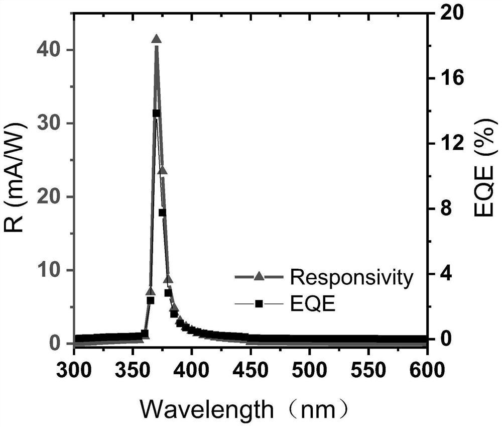
FIG. 4 is a graph of the external quantum efficiency and responsivity of a porous GaN narrow band response UV photodiode of the invention under-2V bias;
FIG. 5 is the specific detectivity of a porous GaN narrow band response ultraviolet photodiode of the present invention;
in the figure, 100-substrate layer, 200-semiconductor layer, 300-porous GaN layer, 400-CuZnS layer, 500-metal contact layer.
Detailed Description
The following further describes embodiments of the present invention with reference to the accompanying drawings:
example 1
As shown in fig. 1 and 2, the present embodiment provides a porous GaN narrowband ultraviolet photodiode, including a substrate layer 100, a semiconductor layer 200, a porous GaN layer 300, a CuZnS layer 400, and a metal contact layer 500, in the present embodiment, the substrate layer 100 is a sapphire substrate layer, the semiconductor layer 200 is disposed on an upper surface of the substrate layer 100, and in the present embodiment, the semiconductor layer 200 is a GaN thin film layer; and the GaN thin film layer has a carrier concentration range of 1 × 10 at room temperature15To 1X 1018cm-3The thickness is 4-6 μm. The semiconductor layer 200 is provided with a porous GaN layer 300 and a CuZnS layer 400, and upper surfaces of the porous GaN layer 300 and the CuZnS layer 400 are provided with a metal contact layer 500. The thickness of the CuZnS layer 400 described in this example is 30-100 nm. The metal contact layer 500 is an ohmic contact layer, and the thickness of the ohmic contact layer is 50-200 nm.
Example 2
The embodiment provides a preparation method of a porous GaN narrow-band ultraviolet photodiode, which comprises the following steps:
s1), depositing a GaN film on the substrate layer 100, wherein the thickness of the deposited GaN film is 5000 nm;
s2), cleaning the GaN film prepared in the step S1), and etching a part of the GaN film by using ionic liquid to form a porous GaN layer 300;
s3), another part of the GaN thin film was treated with a water bath to form a CuZnS layer 400 on the surface, in which the Cu component was 20%.
As preferred in the present embodiment, in step S2), before etching the porous GaN layer 300, 1.0cm × 0.3cm of GaN was placed in aqua regia to remove the passivation layer on the surface, and taken out after five minutes; then, ultrasonically cleaning the GaN sheet in acetone, ethanol and deionized water in sequence, wherein each time is 30 minutes; then, carrying out hydrophilic treatment on the GaN sheet in an ultraviolet ozone cleaning machine to enhance the contact between the GaN sheet and the etching agent, wherein the hydrophilic treatment time is 30 min;
preferably, in step S2), the ionic liquid used is: 1-ethyl-3-methylimidazole trifluoromethanesulfonate.
As preferred in this embodiment, in step S2), the specific preparation method of the porous GaN layer 300 is: using an InGa alloy as an electrode, and enabling the electrode to form ohmic contact with the GaN sheet; the GaN sheet is connected with the positive electrode of a power supply, the platinum sheet is connected with the negative electrode, the two electrodes are placed in parallel and fixed on an iron support, the iron support is placed in the position about 10cm in front of a 300W xenon lamp, and the etched surface of the GaN faces the xenon lamp; soaking the GaN sheet and the platinum sheet in a beaker filled with ionic liquid, setting the voltage of a direct current power supply to be 10V, and etching for 5 min;
preferably, in step S3), the specific method for preparing the CuZnS layer 400 includes: firstly, preparing three precursor solutions:
solution A: 0.06g copper sulfate and 1.68g zinc acetate were mixed in 100ml deionized water; solution B: mixing 0.96g disodium edetate with 100ml deionized water; solution C: 0.6g of C2H5Mixing NS and 100ml deionized water for dissolving;
then mixing the solution B with the solution A and carrying out ultrasonic treatment for 30 min; subsequently, vertically immersing the hydrophilically treated GaN substrate into the mixed solution, and immediately adding the solution C into the mixture; sealing the beaker, heating at 80 deg.C for 60 min.
Example 3
The embodiment provides a preparation method of a porous GaN narrow-band ultraviolet photodiode, which comprises the following steps:
s1), depositing a GaN film on the substrate layer 100, wherein the thickness of the deposited GaN film is 5000 nm;
s2), cleaning the GaN film prepared in the step S1), and etching a part of the GaN film by using ionic liquid to form a porous GaN layer 300;
s3), another part of the GaN thin film was treated with a water bath to form a CuZnS layer 400 on the surface, in which the Cu component was 10%.
As preferred in the present embodiment, in step S2), before etching the porous GaN layer 300, 1.0cm × 0.3cm of GaN was placed in aqua regia to remove the passivation layer on the surface, and taken out after five minutes; then, ultrasonically cleaning the GaN sheet in acetone, ethanol and deionized water in sequence, wherein each time is 30 minutes; then, carrying out hydrophilic treatment on the GaN sheet in an ultraviolet ozone cleaning machine to enhance the contact between the GaN sheet and the etching agent, wherein the hydrophilic treatment time is 30 min;
preferably, in step S2), the ionic liquid used is: 1-ethyl-3-methylimidazole trifluoromethanesulfonate.
As preferred in this embodiment, in step S2), the specific preparation method of the porous GaN layer 300 is: using an InGa alloy as an electrode, and enabling the electrode to form ohmic contact with the GaN sheet; the GaN sheet is connected with the positive electrode of a power supply, the platinum sheet is connected with the negative electrode, the two electrodes are placed in parallel and fixed on an iron support, the iron support is placed in the position about 10cm in front of a 300W xenon lamp, and the etched surface of the GaN faces the xenon lamp; soaking the GaN sheet and the platinum sheet in a beaker filled with ionic liquid, setting the voltage of a direct current power supply to be 10V, and etching for 5 min;
preferably, in step S3), the method for preparing the CuZnS layer 400 includes: firstly, three kinds of precursor solutions are prepared,
solution A: 0.06g copper sulfate and 3.36g zinc acetate were mixed in 200ml deionized water; solution B: mixing and dissolving 1.92g of disodium ethylene diamine tetraacetate and 100ml of deionized water; solution C: 1.2g of C2H5Mixing NS and 100ml deionized water for dissolving;
then mixing the solution B with the solution A and carrying out ultrasonic treatment for 30 min; subsequently, vertically immersing the hydrophilically treated GaN substrate into the mixed solution, and immediately adding the solution C into the mixture; sealing the beaker, heating at 80 deg.C for 60 min.
Example 4
The embodiment provides a preparation method of a porous GaN narrow-band ultraviolet photodiode, which comprises the following steps:
s1), depositing a GaN film on the substrate layer 100, wherein the thickness of the deposited GaN film is 5000 nm;
s2), cleaning the GaN film prepared in the step S1), and etching a part of the GaN film by using ionic liquid to form a porous GaN layer 300;
s3), another part of the GaN thin film was treated with a water bath to form a CuZnS layer 400 on the surface, in which the Cu component was 20%.
As preferred in the present embodiment, in step S2), before etching the porous GaN layer 300, 1.0cm × 0.3cm of GaN was placed in aqua regia to remove the passivation layer on the surface, and taken out after five minutes; then, ultrasonically cleaning the GaN sheet in acetone, ethanol and deionized water in sequence, wherein each time is 30 minutes; then, carrying out hydrophilic treatment on the GaN sheet in an ultraviolet ozone cleaning machine to enhance the contact between the GaN sheet and the etching agent, wherein the hydrophilic treatment time is 30 min;
preferably, in step S2), the ionic liquid used is: 1-ethyl-3-methylimidazole trifluoromethanesulfonate.
As preferred in this embodiment, in step S2), the specific preparation method of the porous GaN layer 300 is: using an InGa alloy as an electrode, and enabling the electrode to form ohmic contact with the GaN sheet; the GaN sheet is connected with the positive electrode of a power supply, the platinum sheet is connected with the negative electrode, the two electrodes are placed in parallel and fixed on an iron support, the iron support is placed in the position about 10cm in front of a 300W xenon lamp, and the etched surface of the GaN faces the xenon lamp; soaking the GaN sheet and the platinum sheet in a beaker filled with ionic liquid, setting the voltage of a direct current power supply to be 15V, and etching for 5 min;
preferably, in step S3), the method for preparing the CuZnS layer 400 includes: firstly, three kinds of precursor solutions are prepared,
solution A: 0.12g copper sulfate and 3.36g zinc acetate were mixed in 200ml deionized water;
solution B: mixing and dissolving 1.92g of disodium ethylene diamine tetraacetate and 100ml of deionized water;
solution C: 1.2g of C2H5Mixing NS and 100ml deionized water for dissolving;
then mixing the solution B with the solution A and carrying out ultrasonic treatment for 30 min; subsequently, vertically immersing the hydrophilically treated GaN substrate into the mixed solution, and immediately adding the solution C into the mixture; sealing the beaker, heating at 80 deg.C for 60 min.
Example 5
In this embodiment, a performance test is performed on the porous GaN narrowband ultraviolet photodiode prepared in embodiment 1, and the light-dark current ratio and other parameters of the ultraviolet photodiode under the irradiation of ultraviolet light at 370nm in a dark place are tested, as can be seen from fig. 3-5, the light-dark current ratio of the device of the ultraviolet photodiode under the irradiation of ultraviolet light at 370nm reaches 585; under the bias of-2V, the prepared photoelectric detector has the peak value responsivity of 41.7mA/W, the peak value external quantum efficiency of 13.86 percent and the detection rate value exceeding 3.78 multiplied by 1012Jones。
As can be seen from the figure, the external quantum efficiency, the responsivity and the detectivity of the prepared porous GaN narrow-band ultraviolet photodiode all obtain a peak value at 370nm of an ultraviolet region, the half-peak width is 5nm, and the response is only generated at 362-388 nm of ultraviolet band, which shows that the prepared device has narrow-band response performance.
The foregoing embodiments and description have been presented only to illustrate the principles and preferred embodiments of the invention, and various changes and modifications may be made therein without departing from the spirit and scope of the invention as hereinafter claimed.
- 上一篇:一种医用注射器针头装配设备
- 下一篇:太阳能电池缓冲层及其制备方法