Solar cell buffer layer and preparation method thereof
阅读说明:本技术 太阳能电池缓冲层及其制备方法 (Solar cell buffer layer and preparation method thereof ) 是由 赵颖 李博研 孙祺 钟大龙 于 2020-05-28 设计创作,主要内容包括:本发明涉及一种太阳能电池缓冲层及其制备方法,所述方法包括将生长基底放入含有锌源、络合剂、硫源和pH调节剂的混合液中进行接触,其中,在所述混合液中,锌源的浓度为0.045-0.08mol/L,锌源、络合剂和硫源的摩尔比为1:(0.75-1.25):(3-8),混合液的pH值为10.3-11。本发明在制备太阳能电池缓冲层的过程中,通过增大锌源浓度,精确控制混合溶液中的锌源、络合剂、硫源和pH调节剂的用量,可以提高Zn(O,S)薄膜的表面质量,降低O/(S+O)比值,从而改善缓冲层与薄膜太阳能电池吸收层界面的匹配性。(The invention relates to a solar cell buffer layer and a preparation method thereof, wherein the method comprises the step of putting a growth substrate into a mixed solution containing a zinc source, a complexing agent, a sulfur source and a pH regulator for contact, wherein in the mixed solution, the concentration of the zinc source is 0.045-0.08mol/L, and the molar ratio of the zinc source to the complexing agent to the sulfur source is 1 (0.75-1.25): (3-8), and the pH value of the mixed solution is 10.3-11. In the process of preparing the solar cell buffer layer, the zinc source concentration is increased, and the dosage of the zinc source, the complexing agent, the sulfur source and the pH regulator in the mixed solution is accurately controlled, so that the surface quality of the Zn (O, S) film can be improved, and the O/(S + O) ratio is reduced, thereby improving the interface matching property of the buffer layer and the absorption layer of the thin-film solar cell.)
1. The solar cell buffer layer is characterized by being a Zn (O, S) thin film, wherein the ratio of O/(S + O) in the Zn (O, S) thin film is 0.6-0.78.
2. The buffer layer of claim 1, wherein the ratio of O/(S + O) in the Zn (O, S) thin film is 0.65-0.75.
3. A preparation method of a buffer layer of a solar cell comprises the steps of putting a growth substrate into a mixed solution containing a zinc source, a complexing agent, a sulfur source and a pH regulator for contact;
wherein, in the mixed solution, the concentration of the zinc source is 0.045-0.08mol/L, the molar ratio of the zinc source to the complexing agent to the sulfur source is 1 (0.75-1.25) to (3-8), and the pH value of the mixed solution is 10.3-11.
4. The preparation method according to claim 3, wherein the concentration of the zinc source in the mixed solution is 0.045-0.06mol/L, and the molar ratio of the zinc source to the complexing agent to the sulfur source is 1 (1-1.15): (3.3-6.7), and the pH value of the mixed solution is 10.5-11.
5. The production method according to claim 3 or 4, wherein the contacting conditions include a contacting temperature of 80 to 95 ℃ and a contacting time of 5 to 30 min.
6. The production method according to any one of claims 3 to 5, wherein the zinc source is at least one selected from the group consisting of zinc nitrate, zinc acetate, zinc oxalate, zinc sulfate and zinc chloride, preferably zinc sulfate.
7. The preparation method according to any one of claims 3 to 6, wherein the complexing agent is selected from at least one of citric acid, sodium citrate, tartaric acid, sodium tartrate, nitrilotriacetic acid, trisodium nitrilotriacetate, preferably sodium citrate.
8. The production method according to any one of claims 3 to 7, wherein the sulfur source is at least one selected from thiourea, thioacetamide, sodium thiosulfate, and preferably thiourea.
9. The production method according to any one of claims 3 to 8, wherein the pH adjuster is at least one selected from the group consisting of sodium hydroxide, aqueous ammonia, hydrazine and hydrazine, preferably aqueous ammonia.
10. A solar cell buffer layer prepared by the method of any one of claims 3-9.
Technical Field
The invention relates to the field of solar cells, in particular to a solar cell buffer layer and a preparation method thereof.
Background
In a CIGS thin-film solar cell, II-VI group compound semiconductor cadmium sulfide (CdS) prepared by a chemical water bath deposition method is generally adopted as a buffer layer. However, the CdS buffer layer contains heavy metal element Cd, so that an operator can easily suck dust and discharged smoke in the manufacturing process, and Cd-containing wastewater discharged in the production process and Cd in waste batteries can pollute the environment, so that the initial investment cost and the operation cost are obviously increased. In addition, the CdS with a smaller forbidden bandwidth (2.4eV) has a strong absorption effect on a visible light short wave part, so that the light transmittance is reduced, and meanwhile, the CdS is doped in an n type, the defect level of the CdS is a deep level defect in the CIGS to form a carrier recombination center, so that the improvement of the current density of the cell is limited. Therefore, there is a need to develop cadmium-free buffer layer materials with higher forbidden band widths and better matching with the CIGS absorber lattice and band gap.
At present, the cadmium-free buffer layer material in the CIGS thin-film solar cell prepared by the mainstream chemical water bath deposition method is Zn (O, S), and the Zn (O, S) is ZnS, ZnO and Zn (OH)2A mixture of (a). Compared with CdS, Zn (O, S) has strong capability of collecting short-wave visible light and high light transmittance. In addition, Zn (O, S) is not only non-toxic and cheap, but also has strong compatibility with existing CdS deposition equipment, so it is considered as the most promising substance to replace CdS as the next generation buffer layer material, and can be rapidly applied industrially.
At present, the process of depositing Zn (O, S) film in chemical water bath usually adopts three mixed solutions of zinc salt, thiourea and ammonia water to form film on the substrate. However, the existing preparation process generally has the following problems: 1) in the preparation process, the consumption of ammonia water is large, the repeatability of a sample is poor, and the burden of waste liquid treatment is heavy; 2) the deposited film has poor quality and more hole defects, and further treatment is needed to improve the quality of the film; 3) the prepared Zn (O, S) has too high proportion of O element and poor matching with a CIGS absorption layer.
The use of ammonia water can be reduced by adding a complexing agent, but the addition of the complexing agent reduces the surface quality of the Zn (O, S) film. Influence of complexing agents on chemical water bath deposition of ZnS films (Liuqi, Shanggong, Aojiaping, functional materials, volume 3 (38) of 2007, 382-385) the influence of different complexing agents (ammonia water, ammonia water-hydrazine and sodium citrate) on chemical water bath deposition of ZnS films was intensively studied, and as a result, it was found that when sodium citrate was used as the complexing agent, the obtained film had a hole defect on the surface and was not suitable for CIGS solar cells.
CN102544237A discloses a preparation method of a buffer layer material of a copper indium gallium selenide thin-film solar cell, when the buffer layer is prepared, 1-10ml of zinc sulfate solution with the concentration of 0.2mol/l is measured firstly, the zinc sulfate solution is added into a 100ml beaker, then 1-3ml of sodium citrate solution with the concentration of 0.1mol/l and 1-3ml of ammonia water with the mass fraction of 25% are added, then a proper amount of deionized water is added, the total volume of the solution in the beaker is made to be 100ml, and finally, 0.46-0.92g of weighed thiourea powder is added into the solution and stirred uniformly. However, the method has the advantages of low zinc sulfate concentration, low water bath temperature, slow deposition rate, long reaction time and poor surface quality of the obtained film. On the SEM image it can be seen that the film surface is either clearly white particles or there are pores that are not completely covered, the surface is rough and the structure is loose.
Therefore, the Zn (O, S) thin film is still to be further improved to improve the electrical properties of the solar cell.
Disclosure of Invention
Aiming at the problem of poor quality of a Zn (O, S) film, the invention provides a solar cell buffer layer and a preparation method thereof. The solar cell buffer layer provided by the invention has the advantages of high surface quality, small O/(S + O) ratio and good matching property with the thin-film solar cell absorption layer interface, and can improve the electrical property of the CIGS solar cell.
In order to solve the above problems, a first aspect of the present invention provides a solar cell buffer layer, which is a Zn (O, S) thin film having a ratio of O/(S + O) of 0.6 to 0.78.
The invention provides a preparation method of a solar cell buffer layer, wherein the method comprises the steps of putting a growth substrate into a mixed solution of a zinc source, a complexing agent, a sulfur source and a pH regulator for contact;
wherein, in the mixed solution, the concentration of the zinc source is 0.045-0.08mol/L, the molar ratio of the zinc source to the complexing agent to the sulfur source is 1 (0.75-1.25) to (3-8), and the pH value of the mixed solution is 10.3-11.
In a third aspect, the invention provides a solar cell buffer layer prepared by the method of the second aspect.
Compared with the prior art, the invention has the following beneficial technical effects:
1) the solar cell buffer layer provided by the invention has good quality, compact film coverage, continuous and uniform distribution, smooth surface without cracks and gaps, and no obvious defects such as attachments, pinholes and the like;
2) in the process of preparing the solar cell buffer layer, the consumption of raw materials, particularly strong-alkaline strong ammonia water, is reduced, so that the production cost, particularly the cost of treating waste liquid containing ammonia water, is reduced;
3) in the process of preparing the solar cell buffer layer, the surface quality of the film can be improved by increasing the concentration of the zinc source and accurately controlling the dosage of the zinc source, the sulfur source, the complexing agent and the pH regulator in the mixed solution, the O/(S + O) ratio is effectively reduced, and a proper band gap is obtained, so that the matching property of the buffer layer and the interface of the absorption layer of the thin film solar cell is improved;
4) according to the preparation method of the solar cell buffer layer, provided by the invention, the buffer layer can be directly used in the device structure of the thin-film solar cell without carrying out more surface treatment after the water bath is finished, so that the production flow is simplified;
5) the preparation method of the solar cell buffer layer provided by the invention has short reaction time and is beneficial to commercial popularization.
Drawings
FIGS. 1 to 10 are SEM images of buffer layers of solar cells prepared in examples 1 to 6 and comparative examples 1 to 4, respectively;
fig. 11 is a graph showing transmittance of buffer layers of solar cells prepared in examples 1 and 2;
fig. 12 to 13 are XPS charts of the buffer layers of the solar cells prepared in examples 1 and 2, respectively.
Detailed Description
The invention provides a solar cell buffer layer, wherein the solar cell buffer layer is a Zn (O, S) thin film, and the ratio of O/(S + O) is 0.6-0.78.
In a preferred embodiment, the ratio of O/(S + O) in the Zn (O, S) thin film is 0.65 to 0.75.
The inventors of the present invention have studied to note that the lattice constant in the Zn (O, S) thin film is linearly related to the content of the S component; the forbidden band width and band edge position of Zn (O, S) are changed along with the change of S content. In order to solve the technical problem of the invention, the inventor of the invention can make the obtained Zn (O, S) film as the buffer layer more matched with the crystal lattice, the band gap and the like of the CIGS absorption layer by controlling the proportional composition of O and S in the chemical water bath deposition Zn (O, S) film, and the prepared solar cell has better photoelectric conversion performance.
The Zn (O, S) film prepared by chemical water bath deposition comprises ZnS, ZnO and Zn (OH)2The O/(O + S) ratio is the percentage of the atomic number of oxygen in the Zn (O, S) film to the sum of the atomic numbers of oxygen and sulfur. The O/(S + O) ratio of the Zn (O, S) film can be tested by an Escalab250Xi type X-ray photoelectron spectrometer under the condition that the excitation source is monochromatized Al Ka (1486.6eV) and the power is 300W.
The second aspect of the invention provides a preparation method of a buffer layer of a solar cell, which comprises the step of putting a growth substrate into a mixed solution of a zinc source, a complexing agent, a sulfur source and a pH regulator for contact, wherein in the mixed solution, the concentration of the zinc source is 0.045-0.08mol/L, the molar ratio of the zinc source to the complexing agent to the sulfur source is 1 (0.75-1.25) to (3-8), and the pH value of the mixed solution is 10.3-11.
The growth substrate in the present invention is a CIGS absorber, which is not particularly limited, and CIGS absorbers commonly used in the art may be used in the present invention. The concentration of the zinc source is measured as the concentration of zinc element contained in the zinc source, the concentration of the sulfur source is measured as the concentration of sulfur element contained in the sulfur source, and the concentration of the complexing agent is measured as the concentration of complexing agent itself.
The inventor of the invention discovers through research that the surface quality of the film can be improved while the use amount of the pH regulator is reduced by increasing the concentration of the zinc source and accurately controlling the contents of the zinc source, the sulfur source, the complexing agent and the pH regulator in the mixed solution, and the O/(S + O) ratio in the Zn (O, S) film is reduced, so that the matching property of the interface of the buffer layer and the absorption layer of the film solar cell is improved.
Wherein, the concentration of the zinc source can be 0.045mol/L, 0.05mol/L, 0.055mol/L, 0.06mol/L, 0.065mol/L, 0.07mol/L, 0.075mol/L and 0.08 mol/L; the ratio of complexing agents may be 0.75, 0.8, 0.85, 0.9, 0.95, 1, 1.05, 1.1, 1.15, 1.2, 1.25; the ratio of the sulfur sources can be 3, 3.3, 3.5, 4, 4.4, 5, 5.5, 6, 6.7, 7, 7.5, 8; the pH of the mixed liquor may be 10.3, 10.4, 10.5, 10.6, 10.7, 10.8, 10.9 and 11.
In a preferred embodiment, the concentration of the zinc source in the mixed solution is 0.045-0.06 mol/L; based on the concentration of the zinc source, the concentration ratio of the zinc source to the complexing agent to the sulfur source is 1 (1-1.15): (3.3-6.7), and the pH value of the mixed solution is 10.5-11.
In a preferred embodiment, zinc sources useful in the art for preparing Zn (O, S) thin films are all applicable in the present invention. Specifically, the zinc source may be selected from at least one of zinc nitrate, zinc acetate, zinc oxalate, zinc sulfate, and zinc chloride, and is preferably zinc sulfate.
In a preferred embodiment, the complexing agent is selected from at least one of citric acid, sodium citrate, tartaric acid, sodium tartrate, nitrilotriacetic acid, trisodium nitrilotriacetate, preferably sodium citrate.
Wherein, the sodium citrate refers to sodium salt of citric acid, and can be trisodium citrate or disodium citrate. Sodium tartrate refers to the sodium salt of tartaric acid, either monosodium tartrate or disodium tartrate.
In a preferred embodiment, sulfur sources useful in the art for preparing Zn (O, S) thin films are all applicable in the present invention. Specifically, the sulfur source is selected from at least one of thiourea, thioacetamide and sodium thiosulfate, and is preferably thiourea.
In a preferred embodiment, the pH adjuster is at least one selected from the group consisting of sodium hydroxide, aqueous ammonia, hydrazine, and preferably aqueous ammonia.
The pH value of the mixed solution mainly influences the hydrolysis degree of the thiourea, and in the invention, the pH regulator is mainly used for regulating the pH value of the mixed solution due to the addition of the complexing agent.
The present invention is not particularly limited in the configuration of the mixed solution, and any method commonly used in the art can be used in the present invention. In a preferred embodiment, the preparation method of the mixed solution comprises the steps of firstly mixing the zinc source and the complexing agent in water, then adding the pH regulator, then adding the sulfur source, and finally adding water to regulate the concentration of the zinc source.
The volume of the mixed solution after the sulfur source is added can basically reach a set value by controlling the water consumption when the zinc source and the complexing agent are mixed, and finally, water is added for fine adjustment to ensure that the total volume of the mixed solution reaches the set value. Because the amount of water added in the final fine adjustment is less, and generally only accounts for 0.2-0.6% of the total volume of the mixed liquor, the influence on the pH value of the mixed liquor is not great, and therefore, the change of the pH value of the mixed liquor after water is added is neglected in the invention.
In a preferred embodiment, the contacting conditions include a contacting temperature of 80-95 ℃, more preferably 80-88 ℃, and a contacting time of 5-30min, more preferably 10-20 min.
Wherein the contact temperature is 80 deg.C, 81 deg.C, 82 deg.C, 83 deg.C, 84 deg.C, 85 deg.C, 86 deg.C, 87 deg.C, 89 deg.C, 90 deg.C, 91 deg.C, 92 deg.C, 93 deg.C, 94 deg.C, 95 deg.C. At present, the process of depositing Zn (O, S) film by chemical water bath is generally carried out at the temperature of about 80 ℃, the deposition temperature is continuously increased, although the reaction rate can be accelerated, the obtained film has poor quality.
The inventor finds that the reason that the poor film forming quality at high temperature is that the excessive reaction temperature accelerates the loss of ammonia gas, destroys the pH environment of the mixed solution, influences the occurrence of deposition reaction, and further reduces the film forming quality, so that cracks are generated on the surface of the film.
However, in the present invention, when the pH regulator is ammonia, the amount of ammonia used in the present invention can be reduced by about 1.6 to 6 times as compared with the prior art ammonia system in which no complexing agent is added. Due to the great reduction of the using amount of the ammonia water, the invention can improve the production efficiency by utilizing high temperature to shorten the reaction time and simultaneously solve the technical problem of poor film forming quality at high temperature.
In addition, the thickness of the film can be adjusted by controlling the reaction time, and in practical application, the thickness of the film can be adjusted according to the content of Ga in the CIGS absorbing layer, so that the matching performance of the buffer layer and the CIGS absorbing layer is better, and the light transmission performance is better.
In a preferred embodiment, the growth substrate is sequentially placed in an organic solvent and deionized water for ultrasonic cleaning before being placed in the mixed solution.
In this case, the present invention is not particularly limited to the cleaning of the growth substrate, and organic solvents and cleaning conditions commonly used in the art can be used in the present invention.
In a preferred embodiment, after the contacting is completed, the growth substrate is removed, washed and dried.
The present invention is not particularly limited to cleaning and drying, and may be carried out by a conventional method in the art. The drying is preferably a nitrogen blow drying. The inventor finds that the high-quality thin film product can be obtained by taking the growth substrate out of the mixed solution, cleaning and drying the growth substrate by nitrogen after the solar cell buffer layer is prepared by the preparation method. The film is uniformly covered on the surface of the growth substrate, has no defects such as cracks and holes, can be used as a buffer layer to be directly used in a device structure of a thin-film solar cell without more surface treatment, and can simplify the production procedure.
In a third aspect, the invention provides a solar cell buffer layer prepared by the method of the second aspect.
In a preferred embodiment, the solar cell buffer layer is a Zn (O, S) thin film, wherein the ratio of O/(S + O) is 0.6 to 0.78.
In a further preferred embodiment, the ratio of O/(S + O) in the Zn (O, S) thin film is 0.65 to 0.75.
In a preferred embodiment, the band gap Eg of the Zn (O, S) thin film is 3.91 to 3.98eV, more preferably 3.94 to 3.95 eV.
The present invention will be described in detail below with reference to specific embodiments thereof, but it should be understood that the scope of the present invention is not limited by the examples.
The thin films prepared in examples 1 to 6 and comparative examples 1 to 4 were analyzed using a Nova Nano450 scanning electron microscope of FEI company, and thickness data of the thin films were measured by a cross-sectional view of SEM. The prepared solar cell buffer layer was subjected to a transmittance test using an ultraviolet visible near infrared spectrophotometer (UV-NIR) (UV 3600 of shimadzu corporation, japan) in a wavelength range of 240-. And (3) performing test calculation on O/(O + S) in a part of Zn (O, S) films by using an Escalab250Xi type X-ray photoelectron spectrometer, wherein the test conditions comprise that an excitation source is monochromated Al K alpha (1486.6eV), and the power is 300W. Since the surface quality of the thin film obtained in the comparative example was too poor to be applied to the sample in the CIGS solar cell, it was selectively subjected to the related performance test in the present invention.
Example 1
1) And respectively cleaning the CIGS absorbing layer serving as a growth substrate in an organic solvent and clear water, wherein the Ga content in the CIGS absorbing layer is about 0.3.
2) Uniformly adding 45mL of 1mol/L zinc sulfate concentrated solution and 45mL of 1mol/L trisodium citrate concentrated solution into 740mL of aqueous solution, then adding ammonia water with the mass fraction of 25% while stirring, and increasing the using amount of the ammonia water according to the real-time pH monitoring value. Then 150mL of 1mol/L thiourea concentrated solution is added, and finally 2-3mL of water is added additionally, so that the total volume of the mixed solution is 1000mL, and the final pH value of the solution is 10.5.
In the obtained mixed solution, the concentration of zinc sulfate is 0.045mol/L, the concentration of sodium citrate is 0.045mol/L, the concentration of thiourea is 0.15mol/L, and the pH value of the mixed solution is 10.5. Wherein the molar ratio of the zinc source, the complexing agent and the sulfur source in the mixed solution is 1: 1: 3.3.
3) and (2) putting the CIGS absorption layer of the growth substrate into a reaction vessel containing a mixed solution for heating reaction, wherein the reaction temperature is 80 ℃, the reaction time is 30min, cooling to room temperature after the reaction is finished, growing a Zn (O, S) cadmium-free buffer layer film on the surface of the CIGS absorption layer, taking out, washing with deionized water, and drying with nitrogen.
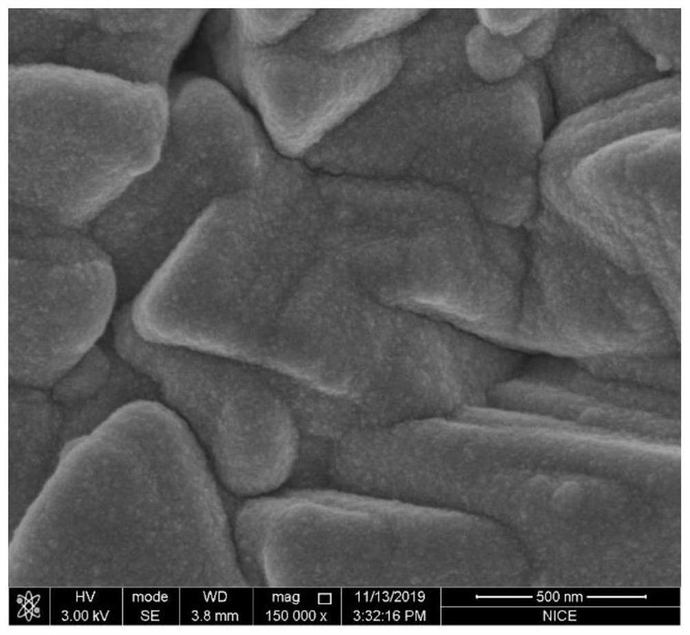
The prepared solar cell buffer layer is observed by an electron microscope, an obtained SEM image is shown in figure 1, and as can be seen from figure 1, the surface of the solar cell buffer layer prepared by the method disclosed by the invention is smooth and has no cracks, has no obvious defects such as attachments, pinholes and the like, the surface quality of a thin film is high, the thin film can be directly used in a device structure of the thin film solar cell without carrying out more surface treatments after water bath is finished, and the production flow is simplified. The film thickness of the thin film was measured to be 65nm by a cross-sectional view of SEM.
And (3) carrying out light transmittance test on the prepared solar cell buffer layer, and carrying out linear fitting on the absorption edge in the transmission spectrum of the sample to obtain the optical band gap of the Zn (O, S) film. The average transmittance of the solar cell buffer layer was 81.61%, and the band gap Eg was 3.95 eV.
In FIG. 12, which is an XPS chart of the buffer layer of the solar cell obtained in example 1, the peak of O1S at 530.4eV is from a Zn-O bond, the peak of O1S at 531.7eV is from a Zn-O-S bond, and the peak of O1S at 533.3eV is from a C-O bond, wherein the peak of C-O represents oxygen contaminated in the environment. And obtaining an O1S fitting curve according to the test result, and calculating the ratio of O/(O + S) in the solar cell buffer layer to be 0.69 by using the O1S fitting curve.
Example 2
The preparation method is the same as example 1, except that: and changing the concentration of the sulfur source to ensure that the molar ratio of the zinc source to the complexing agent to the sulfur source in the mixed solution is 1: 1: 6.7.
the obtained solar cell buffer layer is observed by an electron microscope, and the obtained SEM image is shown in FIG. 2, and as can be seen from FIG. 2, the solar cell buffer layer prepared by the method of the embodiment has smooth surface, no pinhole defects and high film surface quality. The film thickness of the thin film was 80 nm.
And (3) carrying out light transmittance test on the prepared solar cell buffer layer, and carrying out linear fitting on the absorption edge in the transmission spectrum of the sample to obtain the optical band gap of the Zn (O, S) film. The average transmittance of the solar cell buffer layer was 79.77%, and the band gap Eg was 3.95 eV.
FIG. 13 is an XPS chart of the buffer layer of the solar cell prepared in example 2, in FIG. 13, the peak of O1S at 530.4eV is from Zn-O bond, the peak of O1S at 531.7eV is from Zn-O-S bond, and the peak of O1S at 533.3eV is from C-O bond, wherein the peak of C-O represents oxygen contamination in the environment. And obtaining an O1S fitting curve according to the test result, and calculating the ratio of O/(O + S) in the solar cell buffer layer to be 0.68 by using the O1S fitting curve.
Fig. 11 is a graph showing transmittance of buffer layers of solar cells prepared in examples 1 and 2.
Example 3
The preparation method is the same as example 1, except that: the concentration of the zinc source is 0.06 mol/L.
The prepared solar cell buffer layer is observed by an electron microscope, and an obtained SEM image is shown in figure 3, compared with figure 1, the film is uniform and continuous, large particles in a visual field range are almost absent, and the surface quality of the film is better.
And (3) carrying out light transmittance test on the prepared solar cell buffer layer, and carrying out linear fitting on the absorption edge in the transmission spectrum of the sample to obtain the optical band gap of the Zn (O, S) film. The average transmittance of the solar cell buffer layer was 81.8%, and the band gap Eg was 3.95 eV.
The prepared solar cell buffer layer was subjected to XPS testing, wherein the ratio of O/(O + S) in the solar cell buffer layer was 0.69.
Example 4
The preparation method is the same as example 1, except that: the pH of the mixture was 10.3.
The obtained solar cell buffer layer was observed by an electron microscope, and the obtained SEM image is shown in fig. 4, and it can be seen from fig. 4 that: the film is uniformly distributed on the absorption layer, the surface has no pinholes or cracks, and has no white particles, and the surface quality is high. The film thickness of the thin film was 53 nm.
The prepared solar cell buffer layer was subjected to XPS testing, wherein the ratio of O/(O + S) in the solar cell buffer layer was 0.71.
Example 5
The preparation method is the same as example 1, except that: pH of the mixture was 11.
The prepared solar cell buffer layer is observed by an electron microscope, and an SEM image is shown in FIG. 5, and the surface quality is high. The film thickness of the thin film was 28 nm.
The prepared solar cell buffer layer was subjected to XPS testing, wherein the ratio of O/(O + S) in the solar cell buffer layer was 0.67.
Example 6
The preparation method is the same as example 1, except that: the reaction temperature was 88 ℃ and the reaction time was 20 min.
The prepared solar cell buffer layer is observed by an electron microscope, an obtained SEM image is shown in FIG. 6, the SEM image is obviously observed from FIG. 6, no crack is generated on the surface of the thin film obtained by contacting at high temperature, the thin film is uniformly distributed, and the film forming quality is high. The film thickness of the thin film was 31 nm.
And (3) carrying out light transmittance test on the prepared solar cell buffer layer, and carrying out linear fitting on the absorption edge in the transmission spectrum of the sample to obtain the optical band gap of the Zn (O, S) film. The average transmittance of the solar cell buffer layer was 83.99%, and the band gap Eg was 3.94 eV.
The prepared solar cell buffer layer was subjected to XPS testing, wherein the ratio of O/(O + S) in the solar cell buffer layer was 0.69.
Comparative example 1
The preparation method is the same as example 1, except that: the concentration of the zinc source is 0.03 mol/L.
The prepared solar cell buffer layer was observed by an electron microscope, and the obtained SEM image is shown in fig. 7. Although the thickness of the buffer layer of the solar cell reaches 60nm, the content of each component in the mixed solution is low due to the low concentration of the zinc source, the formed film has poor uniformity, rough surface, loose structure, pinholes, discontinuity, poor quality and unsuitability for the CIGS solar cell because the film does not cover the whole film surface.
Comparative example 2
The preparation method is the same as example 1, except that: and changing the concentrations of the complexing agent and the sulfur source to ensure that the concentration ratio of the zinc source to the complexing agent to the sulfur source in the mixed solution is 1: 2: 3.3.
the prepared solar cell buffer layer was observed by an electron microscope, and the obtained SEM image is shown in fig. 8. As can be seen from fig. 8, in comparative example 2, increasing the concentration of the complexing agent, causing a large number of pinhole defects on the surface, the thin film is not dense, and the non-dense buffer layer cannot completely cover the absorber layer, which may result in a significant decrease in efficiency or even failure of the CIGS solar cell device, although the obtained Zn (O, S) thin film has a film thickness of 30nm and an average transmittance of 82.81%, the surface quality is too poor to be applied to the CIGS solar cell.
Comparative example 3
The preparation method is the same as example 1, except that: and changing the concentration of the sulfur source to ensure that the concentration ratio of the zinc source to the complexing agent to the sulfur source in the mixed solution is 1: 1: 15.
the prepared solar cell buffer layer is observed by an electron microscope, and the obtained SEM image is shown in FIG. 9. As is clear from FIG. 9, in comparative example 3, when the amount of the sulfur source added was increased, the resulting film had uneven surface and a large number of white particles, and the film was analyzed by EDS to be ZnO or Zn (OH)2The particles are harmful to the CIGS solar cell, can reduce the conversion efficiency of the CIGS solar cell, is not beneficial to the preparation of a subsequent magnetron sputtering window layer thin film, has poor quality and is not suitable for the CIGS solar cell.
Comparative example 4
The preparation method is the same as example 1, except that: the pH of the mixture was 10.
The prepared solar cell buffer layer was observed by an electron microscope, and the obtained SEM image is shown in fig. 10. As can be seen from fig. 10, in comparative example 4, the amount of ammonia water was reduced, so that white particles on the surface of the thin film were increased and the quality was degraded, and although the film thickness of the buffer layer of the solar cell was 32nm, the photoelectric conversion performance of the solar cell thus manufactured was low.
The above description is only for the preferred embodiment of the present invention, but the scope of the present invention is not limited thereto, and those skilled in the art can easily conceive of the changes or substitutions within the technical scope of the present invention. Therefore, the protection scope of the present invention shall be subject to the protection scope of the claims.
- 上一篇:一种医用注射器针头装配设备
- 下一篇:一种双结薄膜太阳能电池及其制作方法